|
|
马上注册,结交更多好友,享用更多功能,让你轻松玩转社区
您需要 登录 才可以下载或查看,没有账号?立即注册
×
<strong>10 observations from SPIE Litho
</strong>Mark LaPedus, Dylan McGrath
EE Times
(02/26/2010 1:34 PM EST)
SAN JOSE, Calif. -- The themes of this year's SPIE Advanced Lithography event were clear: ''D and D.'' That stands for delays and double-patterning. Indeed, EUV is delayed. So is maskless. And nano-imprint is still stuck in R&D. So, chip makers must continue to ride the 193-nm immersion wave. They must also look at dreaded double-patterning techniques. In any case, here's what <i>EE Times</i> observed at SPIE: <strong>1. EUV woes.</strong> Extreme ultraviolet (EUV) lithography is delayed--again. Now, the industry faces dreaded double-patterning or some variation of the technology to extend 193-nm immersion. That article can be read here. <strong>2. Self-assembly grabs the spotlight.</strong> If there is a darling of this year's SPIE, it just might be directed self-assembly, a technology that emerged in recent years to land on the International Technology Roadmap for Semiconductors (ITRS) and is considered a potential candidate to extend optical lithography. That article can be read here. <strong>3. Direct-write litho still facing uphill climb.</strong> At least according to one prominent lithography researcher, multi-beam production tools are still a minimum of five years away. That article can be read here. <strong>4. Nano-imprint still stuck in R&D.</strong> While nano-imprint has not cracked mainstream production in semiconductor fabs, as some had hoped at one time, the technology has been delayed in perhaps its biggest potential market: hard disk drives (HDDs). That article can be read here. <strong>5. Tool vendors are cautious despite the upturn.</strong> The fab tool market is ''hot'' and litho vendors are seeing lead times stretch out to 15 months for new orders, said G. Dan Hutcheson, CEO of market research firm VLSI Technology Inc. Still, vendors are worried. Why? ''The market is recovering. Last year, we were at the bottom and it was scary. It's not quite time to celebrate,'' said Hamid Zarringhalam, vice president of technical sales and marketing at Nikon Precision Inc. ''Things are looking better. We are seeing growth. But it will take time to fully recover.'' Another tool vendor sees a ''double dip'' coming. Others still see more technology buys verses capacity buys. <strong>6. Where's the booths?</strong> The SPIE event itself seemed smaller than last year, but attendance was OK. Missing at the event were the booths of the big name players. Applied, ASML, Canon and Nikon did not have booths. So foot traffic in the exhibition hall was light. OK. It was a ghost town. <strong>7. Let's laugh a little.</strong> Let's face it: SPIE is sometimes dry and boring. However, TSMC tried to change the mood. During a presentation, TSMC attempted to convince the audience that EUV is cheaper than double-patterning. In a chart, it proved its point. The trouble: TSMC neglected to add EUV mask costs to the equation, meaning its data was wrong and pointless. It did draw some much needed laughter during the dry event. Thanks for the memories, TSMC. <strong>8. M&A in the air?</strong> We get the feeling it's a make-or-break year for some litho vendors. IMS, Mapper, MII and others must show more progress--or else. Consolidation appears to be in the air. Our feeling: ASML could enter the nano-imprint field, which could shake up the landscape. <strong>9. We want to party!</strong> There were fewer receptions this year. Nikon had its event. Canon did not have its party. Brion, now part of ASML, did not hold its annual event. ASML had a party for customers, but it was not open to the media. To be honest, SPIE was a gloomy event. <strong>10. No time to party.</strong> On the other hand, there's too much to cover at SPIE (i.e. EUV, ML2, nano-imprint, self-assembly, etc.). So we have little or no time for the receptions or parties. (Ok. Maybe one or two). |
|


 再发某公司的PADS格式 PCB封装库全套共享
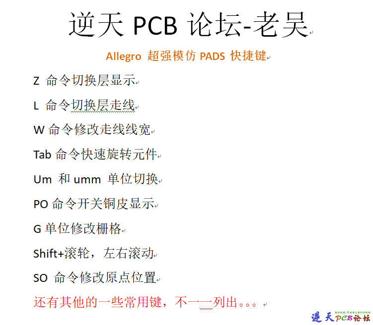 Allegro超强最全模仿PADS快捷键实现Z切换层
 28550975PCB 28550975PCB
 02-718-611 02-718-611
 YT8531C +PI6C557-03BLE 做的RK3568 底板PC
 新塘 NuMaker-IoT-MA35D0-A1_202505 参考板
 CT7601-EVM-G-A-V10评估板PCB原理图应用说
 allegro羊皮卷
 iphone6s的PCB文件(PADS格式)
 晶晨S905X5带单片LPDDR5参考设计,ORCAD+PAD
 抗干扰1通道/1键触摸触控检测芯片超小封装
 高速数字设计-霍华德.约翰逊著 沈立 朱来
 IPC-TM-650中文版.pdf
 AutoCAD 安装包大全 百度网盘


 发表于 2013-3-30 00:13:11

")
")