|
|
马上注册,结交更多好友,享用更多功能,让你轻松玩转社区
您需要 登录 才可以下载或查看,没有账号?立即注册
×
<strong>
</strong><strong></strong><strong></strong><strong></strong><strong></strong><strong></strong><strong></strong><strong></strong> Mark LaPedus
EE Times
(02/23/2010 5:02 PM EST)
SAN JOSE, Calif. -- The eBeam Initiative--a forum dedicated to the education and promotion of a new design-to-manufacturing approach known as design for e-beam (DFEB)--has announced that six additional companies have joined the group. New members in the Initiative include the following firms: GlobalFoundries, JEOL, KLA-Tencor, NuFlare Technology, Petersen Advanced Lithography (PAL) and Samsung Electronics. The eBeam Initiative was launched last year. The effort initially had 20 companies from across the chip spectrum, including EDA vendors, ASIC suppliers, makers of e-beam tools, photomask suppliers and others. The group is lead by Direct2Silicon Inc. (D2S) and guided by a formal steering committee that includes Advantest, CEA/Leti, e-Shuttle, Fujitsu Microelectronics and Vistec. The semiconductor industry has long been interested in applications of direct-write e-beam technology, which removes costly photomask sets from the equation and enables patterning of circuitry directly on a wafer. Separately, D2S rolled out its new design for e-beam (DFEB) mask technology for the production of advanced optical photomasks with circular and curvilinear shapes. Used in conjunction with currently available e-beam mask writing equipment, D2S DFEB mask technology reduces the write times for masks containing complex or curvilinear features to enable the extension of 193-nm immersion lithography to the 22-nm node and beyond with practical turnaround time. "This announcement is the latest step in our goal of continuous innovation in order to bridge the gap between design and manufacturing with e-beam technologies," stated Aki Fujimura, president and CEO of D2S, in a statement. "D2S can bring the advantages of our DFEB mask technology to high-volume, leading-edge semiconductor manufacturing applications--and with that we can help the semiconductor industry realize the possibility of cost-effective optical lithography at the 22-nm node." |
|

 再发某公司的PADS格式 PCB封装库全套共享
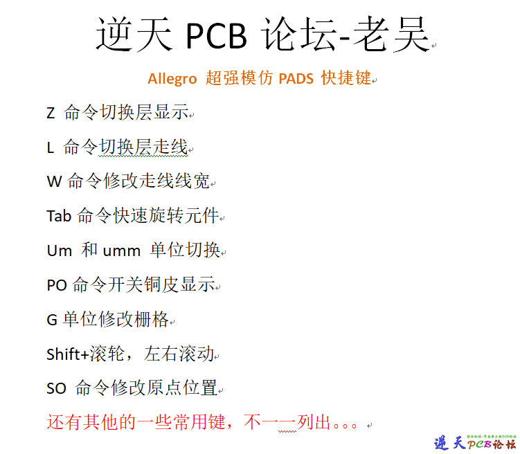 Allegro超强最全模仿PADS快捷键实现Z切换层
 TL6678F-EasyEVM-PCI Express x4连接器-SFP
 TL5728-IDK-A3_16D2六路以太网
 TL5728F-EVM-A2_16D2-SFP接口
 君正T20 原厂DEMO板PCB文件
 Intel JSL平台笔记本主板
 allegro羊皮卷
 台灯/风扇触摸IC/高抗干扰触摸芯片/4路/4键
 Altium_Designer_14电路设计与仿真.pdf 高
 (抢先版)Cadence Allegro17.4羊皮卷
 汽车雷达回波发生器的技术原理和应用场景
 永嘉微电LCD驱动原厂/高抗噪LCD驱动IC/段码
 Python首次超越Java成第二最受欢迎的编程语


 发表于 2013-3-30 00:11:05

")
")