|
|
马上注册,结交更多好友,享用更多功能,让你轻松玩转社区
您需要 登录 才可以下载或查看,没有账号?立即注册
×
Micron gears up for sub-25nm NAND technology, EZ-NAND solutionsPrinter friendly
Related stories
Comments
Email to a friend
Latest news
Josephine Lien, Taipei; Jessie Shen, DIGITIMES [Tuesday 2 March 2010]
Micron Technology is set to advance its NAND flash process technology to sub-25nm nodes in 2011, and is gearing up the development of NAND memory supporting ONFI's soon-to-be available specification called EZ-NAND, according to Kevin Kilbuck, director of NAND market development for Micron.
According to Micron's NAND flash process roadmap, the company expects to enter the sub-25nm technology era in 2011 about one year after mass production of 25nm-made products in mid-2010. The memory maker also looks to develop its charge trap flash (CTF) technology, a replacement option for the current mainstream floating-gate NAND technology.
In terms of applications, Micron has offered managed NAND portfolio that supports the eMMC standard for handset and GPS navigator applications, Kilbuck said. eMMC solutions, seen as an alternative to NOR flash, provide a standard interface specification that minimizes the need for host software to accommodate process node migrations and different chipmakers' NAND flash devices.
Micron is also vying for a piece of the market for portable and consumer electronics applications. Kilbuck revealed the company's plan to introduce new NAND solutions that will feature the EZ-NAND specification. The new chips will operate more like storage media, with an 8Gb device capable of storing 2,000 songs or 7,000 photos like a DVD storage.
ONFI recently announced it has begun work on the new technology specification, which is expected to be completed in the mid-2010 timeframe. EZ-NAND is to build ECC (error checking and correction) into the NAND die rather than the system, which will remove the burden of the host controller to keep pace with the fast-changing ECC requirements of NAND technology. |
|

 再发某公司的PADS格式 PCB封装库全套共享
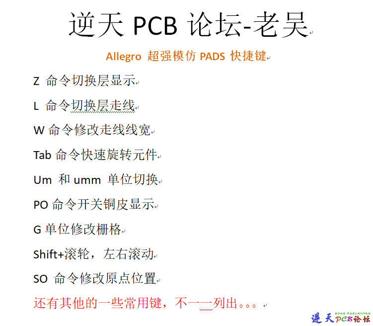 Allegro超强最全模仿PADS快捷键实现Z切换层
 TL6678F-EasyEVM-PCI Express x4连接器-SFP
 TL5728-IDK-A3_16D2六路以太网
 TL5728F-EVM-A2_16D2-SFP接口
 君正T20 原厂DEMO板PCB文件
 Intel JSL平台笔记本主板
 allegro羊皮卷
 台灯/风扇触摸IC/高抗干扰触摸芯片/4路/4键
 Altium_Designer_14电路设计与仿真.pdf 高
 (抢先版)Cadence Allegro17.4羊皮卷
 汽车雷达回波发生器的技术原理和应用场景
 永嘉微电LCD驱动原厂/高抗噪LCD驱动IC/段码
 Python首次超越Java成第二最受欢迎的编程语


 发表于 2013-3-30 00:15:51

")
")