|
|
马上注册,结交更多好友,享用更多功能,让你轻松玩转社区
您需要 登录 才可以下载或查看,没有账号?立即注册
×
<div><p style="margin-bottom: 12px; padding: 0px; word-wrap: break-word; letter-spacing: 0.5px; font-size: 16px; background-color: rgb(255, 255, 255); text-indent: 2em; color: rgb(51, 51, 51) !important; line-height: 30px !important; font-family: "Microsoft yahei", 微软雅黑 !important;">众人一讲到半导体高端技术,第一个联想到的是ASML的光刻机,但真正让台积电狠甩<a href="http://www.elecfans.com/tags/%E4%B8%89%E6%98%9F/" target="_blank" style="cursor: pointer; text-decoration-line: none; color: rgb(66, 152, 186); word-break: break-all;"><u>三星</u></a>电子(S<a href="http://www.elecfans.com/tags/ams/" target="_blank" style="cursor: pointer; text-decoration-line: none; color: rgb(66, 152, 186); word-break: break-all;"><u>ams</u></a>ungElectronics)几条街,大啖苹果(Apple)订单的关键,却是来自于半导体界最末端的“传统产业”:封装技术,台积电进入该领域晚于三星,但从此由前段制程吃到后段工艺,这种一条龙的技术与服务宛若“神奇大补丸”,从此苹果离不开它!</p><p style="margin-bottom: 12px; padding: 0px; word-wrap: break-word; letter-spacing: 0.5px; font-size: 16px; background-color: rgb(255, 255, 255); text-indent: 2em; color: rgb(51, 51, 51) !important; line-height: 30px !important; font-family: "Microsoft yahei", 微软雅黑 !important;">更让竞争对手竖起寒毛的是,台积电在今年首度揭露一种全新的封装架构,同时也赋予一个独特名字:“SoIC”(sys<a href="http://www.elecfans.com/tags/te/" target="_blank" style="cursor: pointer; text-decoration-line: none; color: rgb(66, 152, 186); word-break: break-all;"><u>te</u></a>m-on-integrated-chips)。然该技术细节一公布,业界便议论纷纷指出,“这不就十分接近3DIC架构吗?”,业内人士指出,台积电从来都是“事做成了才会说”,这次敢公开讲这个技术,一定是有十足把握才会提。</p><p style="margin-bottom: 12px; padding: 0px; word-wrap: break-word; letter-spacing: 0.5px; font-size: 16px; background-color: rgb(255, 255, 255); text-indent: 2em; color: rgb(51, 51, 51) !important; line-height: 30px !important; font-family: "Microsoft yahei", 微软雅黑 !important;"><strong>3DIC是半导体“至尊”殿堂,这一把剑台积电磨了超过十年</strong></p><p style="margin-bottom: 12px; padding: 0px; word-wrap: break-word; letter-spacing: 0.5px; font-size: 16px; background-color: rgb(255, 255, 255); text-indent: 2em; color: rgb(51, 51, 51) !important; line-height: 30px !important; font-family: "Microsoft yahei", 微软雅黑 !important;">3DIC技术已经被半导体业界讨论多年,但难度十分高,是透过高度的堆叠来整合不同性质的晶圆,有别于2.5D封装是不同的Die(晶粒)在基板上做平行排列,其技术层次是半导体界的“至尊”殿堂。</p><p style="margin-bottom: 12px; padding: 0px; word-wrap: break-word; letter-spacing: 0.5px; font-size: 16px; background-color: rgb(255, 255, 255); text-indent: 2em; color: rgb(51, 51, 51) !important; line-height: 30px !important; font-family: "Microsoft yahei", 微软雅黑 !important;">而台积电这次提出的接近3DIC架构的“SoIC”技术绝非是横空出世,甚至可说是“历经磨难”才找到的“桃花源”,这一把剑磨了可不止十年。</p><p style="margin-bottom: 12px; padding: 0px; word-wrap: break-word; letter-spacing: 0.5px; font-size: 16px; background-color: rgb(255, 255, 255); text-indent: 2em; color: rgb(51, 51, 51) !important; line-height: 30px !important; font-family: "Microsoft yahei", 微软雅黑 !important;">SoIC是一种创新的多晶片堆叠技术,主要是针对10nm以下的工艺技术进行晶圆级接合,特色是SoIC技术没有突起的键合结构,是一种直接W<a href="http://www.elecfans.com/tags/afe/" target="_blank" style="cursor: pointer; text-decoration-line: none; color: rgb(66, 152, 186); word-break: break-all;"><u>afe</u></a>r-on-wafer的接合技术,可以把很多不同性质的芯片整合在一起,而当中最关键之处,是在于接合的材料。</p><p style="margin-bottom: 12px; padding: 0px; word-wrap: break-word; letter-spacing: 0.5px; font-size: 16px; background-color: rgb(255, 255, 255); text-indent: 2em; color: rgb(51, 51, 51) !important; line-height: 30px !important; font-family: "Microsoft yahei", 微软雅黑 !important;">台积电掌舵IntegratedInterconnect& ackaging部门的副总余振华提到SoIC技术时透露,Wafer-on-wafer接合的材料是个“billiondolla<a href="http://www.elecfans.com/tags/rs/" target="_blank" style="cursor: pointer; text-decoration-line: none; color: rgb(66, 152, 186); word-break: break-all;"><u>rs</u></a>”的秘密!</p><p style="margin-bottom: 12px; padding: 0px; word-wrap: break-word; letter-spacing: 0.5px; font-size: 16px; background-color: rgb(255, 255, 255); text-indent: 2em; color: rgb(51, 51, 51) !important; line-height: 30px !important; font-family: "Microsoft yahei", 微软雅黑 !important;">同时,近期台积电首度揭露SoIC封装技术的最新进展时间表,将在从2020年起为台积电贡献营收,并将在2021年创造显著收入贡献。</p><p style="margin-bottom: 12px; padding: 0px; word-wrap: break-word; letter-spacing: 0.5px; font-size: 16px; background-color: rgb(255, 255, 255); text-indent: 2em; color: rgb(51, 51, 51) !important; line-height: 30px !important; font-family: "Microsoft yahei", 微软雅黑 !important;">回顾过往,台积电的封装技术之路是几经波折,先是提出2.5D版的CoWos技术,再提出横扫市场且独吃苹果的InFO技术,下一个要制霸的,是逼近3DIC层次的SoIC技术。</p><p style="margin-bottom: 12px; padding: 0px; word-wrap: break-word; letter-spacing: 0.5px; font-size: 16px; background-color: rgb(255, 255, 255); text-indent: 2em; color: rgb(51, 51, 51) !important; line-height: 30px !important; font-family: "Microsoft yahei", 微软雅黑 !important;"><strong>10年前超低调成立封装部门,就怕合作伙伴抱怨“抢饭碗”</strong></p><p style="margin-bottom: 12px; padding: 0px; word-wrap: break-word; letter-spacing: 0.5px; font-size: 16px; background-color: rgb(255, 255, 255); text-indent: 2em; color: rgb(51, 51, 51) !important; line-height: 30px !important; font-family: "Microsoft yahei", 微软雅黑 !important;">台积电在2008年底成立导线与封装技术整合部门(IntegratedInterconnectandPackageDevelopmentDivision,IIPD),要进军封装领域和合作伙伴“抢饭碗”的消息不胫而走,一度看在封测业者的眼里是很不是滋味。</p><p style="margin-bottom: 12px; padding: 0px; word-wrap: break-word; letter-spacing: 0.5px; font-size: 16px; background-color: rgb(255, 255, 255); text-indent: 2em; color: rgb(51, 51, 51) !important; line-height: 30px !important; font-family: "Microsoft yahei", 微软雅黑 !important;">封测产业被半导体界视为是高端技术领域中的“传统产业”,在专业分工缜密的行业特性下,封测业的运营型态一直是非常成熟传统、低毛利率,与台积电擅长的技术密集、资本密集、高毛利率是大相径庭。</p><p style="margin-bottom: 12px; padding: 0px; word-wrap: break-word; letter-spacing: 0.5px; font-size: 16px; background-color: rgb(255, 255, 255); text-indent: 2em; color: rgb(51, 51, 51) !important; line-height: 30px !important; font-family: "Microsoft yahei", 微软雅黑 !important;">然而,台积电为什么要进入封装领域?因为早在10年前,公司就看出,随着工艺不断往下微缩,后段封装技术会跟不上前段制程,如此发展会拖累台积电开发高端技术的速度,而摩尔定律撞墙的预言也会成真,唯一解决之道就是从前段到后段一条龙做到底,自己打通任督二脉。</p><p style="margin-bottom: 12px; padding: 0px; word-wrap: break-word; letter-spacing: 0.5px; font-size: 16px; background-color: rgb(255, 255, 255); text-indent: 2em; color: rgb(51, 51, 51) !important; line-height: 30px !important; font-family: "Microsoft yahei", 微软雅黑 !important;">当然,另一个让台积电如鲠在喉的理由,是主要竞争对手三星早已采用从前段做到后段的模式,因此,跨入封测产业成为台积电势在必行的策略,但初期又必须非常小心翼翼,深怕合作伙伴过度反弹。</p><p style="margin-bottom: 12px; padding: 0px; word-wrap: break-word; letter-spacing: 0.5px; font-size: 16px; background-color: rgb(255, 255, 255); text-indent: 2em; color: rgb(51, 51, 51) !important; line-height: 30px !important; font-family: "Microsoft yahei", 微软雅黑 !important;"><strong>为了“咬一口苹果”,与三星上演“顶尖对决”戏码</strong></p><p style="margin-bottom: 12px; padding: 0px; word-wrap: break-word; letter-spacing: 0.5px; font-size: 16px; background-color: rgb(255, 255, 255); text-indent: 2em; color: rgb(51, 51, 51) !important; line-height: 30px !important; font-family: "Microsoft yahei", 微软雅黑 !important;">台积电在2008年成立导线与封装技术整合部门后的第一个任务,是将超低介电层(ExtremeLow-KDielectric,ELK)导入45/40纳米工艺技术,接着突破导线与封装相关技术瓶颈,让第一批<a href="http://www.elecfans.com/tags/gpu/" target="_blank" style="cursor: pointer; text-decoration-line: none; color: rgb(66, 152, 186); word-break: break-all;"><u>GPU</u></a>和<a href="http://www.elecfans.com/tags/fpga/" target="_blank" style="cursor: pointer; text-decoration-line: none; color: rgb(66, 152, 186); word-break: break-all;"><u>FPGA</u></a>客户的产品顺利量产。</p><p style="margin-bottom: 12px; padding: 0px; word-wrap: break-word; letter-spacing: 0.5px; font-size: 16px; background-color: rgb(255, 255, 255); text-indent: 2em; color: rgb(51, 51, 51) !important; line-height: 30px !important; font-family: "Microsoft yahei", 微软雅黑 !important;">当台积电进入封装领域,又全力押宝手机应用,与劲敌三星电子之间的“顶尖对决”一役火热上演,在争夺苹果处理器订单上达到高潮。</p><p style="margin-bottom: 12px; padding: 0px; word-wrap: break-word; letter-spacing: 0.5px; font-size: 16px; background-color: rgb(255, 255, 255); text-indent: 2em; color: rgb(51, 51, 51) !important; line-height: 30px !important; font-family: "Microsoft yahei", 微软雅黑 !important;">苹果第一颗iPhone处理器是2010年问世的A4芯片,之后的A5、A6、A7芯片都是由三星打造,然三星在智能手机领域的强势拓展,对苹果iPhone的威胁越来越大,演变成双方互告专利侵权是吵得面红耳赤。</p><p style="margin-bottom: 12px; padding: 0px; word-wrap: break-word; letter-spacing: 0.5px; font-size: 16px; background-color: rgb(255, 255, 255); text-indent: 2em; color: rgb(51, 51, 51) !important; line-height: 30px !important; font-family: "Microsoft yahei", 微软雅黑 !important;">因此,2011年就传出苹果秘密与台积电接触,讨论代工处理器一事,此举引发三星十分激烈的反击,开始私下四处找分析师放话表示,台积电的技术还不够成熟、相关专利都在三星手上,只要台积电敢做一定告到底等。</p><p style="margin-bottom: 12px; padding: 0px; word-wrap: break-word; letter-spacing: 0.5px; font-size: 16px; background-color: rgb(255, 255, 255); text-indent: 2em; color: rgb(51, 51, 51) !important; line-height: 30px !important; font-family: "Microsoft yahei", 微软雅黑 !important;">当时就盛传苹果的A6处理器会从三星转到台积电,但最后仍是由三星代工,韩国媒体还形容“因为台积电做不出A6芯片,让苹果只能接受三星大涨价格且继续合作”。</p><p style="margin-bottom: 12px; padding: 0px; word-wrap: break-word; letter-spacing: 0.5px; font-size: 16px; background-color: rgb(255, 255, 255); text-indent: 2em; color: rgb(51, 51, 51) !important; line-height: 30px !important; font-family: "Microsoft yahei", 微软雅黑 !important;">但事实上,苹果与台积电这对“新朋友”从接触认识到真正合作,花了很长的时间沟通与磨合。</p><p style="margin-bottom: 12px; padding: 0px; word-wrap: break-word; letter-spacing: 0.5px; font-size: 16px; background-color: rgb(255, 255, 255); text-indent: 2em; color: rgb(51, 51, 51) !important; line-height: 30px !important; font-family: "Microsoft yahei", 微软雅黑 !important;"><strong>台积电、苹果磨合三年,A8处理器横空出世</strong></p><p style="margin-bottom: 12px; padding: 0px; word-wrap: break-word; letter-spacing: 0.5px; font-size: 16px; background-color: rgb(255, 255, 255); text-indent: 2em; color: rgb(51, 51, 51) !important; line-height: 30px !important; font-family: "Microsoft yahei", 微软雅黑 !important;">为了争取苹果订单,台积电2011年底就组织一批将近百人的研发团队长期驻扎美国苹果总部,但是一直到2014年,台积电以20纳米为苹果打造A8处理器才真正量产问世,中间磨合了三年,传出有两大原因。</p><p style="margin-bottom: 12px; padding: 0px; word-wrap: break-word; letter-spacing: 0.5px; font-size: 16px; background-color: rgb(255, 255, 255); text-indent: 2em; color: rgb(51, 51, 51) !important; line-height: 30px !important; font-family: "Microsoft yahei", 微软雅黑 !important;">一是要先解决专利问题,三星因为握有许多逻辑、存储等相关专利,是绑住苹果订单的一大诱因,且为求谨慎,台积电也花了更长的时间通过苹果的的认证,双方确保所有矽智财都不会有侵权的疑虑,苹果才正式转单给台积电。</p><p style="margin-bottom: 12px; padding: 0px; word-wrap: break-word; letter-spacing: 0.5px; font-size: 16px; background-color: rgb(255, 255, 255); text-indent: 2em; color: rgb(51, 51, 51) !important; line-height: 30px !important; font-family: "Microsoft yahei", 微软雅黑 !important;">第二个原因,传出就是因为台积电后段封装制程不够稳定,成了争取苹果订单最大的绊脚石,逼得台积电在2011年底,首次将封装技术COWOS(ChipOnWaferOnSubstrate)这个秘密武器在众人面前揭露,从此,台积电在封装领域上的一举一动,成了业界关注的焦点,不单是竞争对手三星紧紧盯着,所有封测业者都也张大眼睛瞧着。</p><p style="margin-bottom: 12px; padding: 0px; word-wrap: break-word; letter-spacing: 0.5px; font-size: 16px; background-color: rgb(255, 255, 255); text-indent: 2em; color: rgb(51, 51, 51) !important; line-height: 30px !important; font-family: "Microsoft yahei", 微软雅黑 !important;">之后剧本发展更是大转弯,后段的封装技术不足,原本是台积电争取苹果A6处理器输给三星的原因,但自从在A8处理器订单大获全胜后,台积电的封测技术反而成为击败三星、独吃苹果订单的秘技,对照台积电超过30年的发展史,一个2008年才成立的年轻部门,却为台积电打赢极为漂亮的一仗!</p><p style="margin-bottom: 12px; padding: 0px; word-wrap: break-word; letter-spacing: 0.5px; font-size: 16px; background-color: rgb(255, 255, 255); text-indent: 2em; color: rgb(51, 51, 51) !important; line-height: 30px !important; font-family: "Microsoft yahei", 微软雅黑 !important;">台积电的封装分为两大技术,一是专注于高阶客户市场的整合型扇出封装CoWoS封装技术,二是经济型InFO(IntegratedFan-out)技术。</p><p style="margin-bottom: 12px; padding: 0px; word-wrap: break-word; letter-spacing: 0.5px; font-size: 16px; background-color: rgb(255, 255, 255); text-indent: 2em; color: rgb(51, 51, 51) !important; line-height: 30px !important; font-family: "Microsoft yahei", 微软雅黑 !important;">CoWoS封装技术最先搬上台面,虽然市场好评不断,但因为价格较高,只能锁定部分高端用户,像是GPU、FPGA等应用,台积电马上修正策略,主打经济版的InFO封装技术,遂成为手机客户采用的主力,也是独吃苹果订单的关键。</p><p style="margin-bottom: 12px; padding: 0px; word-wrap: break-word; letter-spacing: 0.5px; font-size: 16px; background-color: rgb(255, 255, 255); text-indent: 2em; color: rgb(51, 51, 51) !important; line-height: 30px !important; font-family: "Microsoft yahei", 微软雅黑 !important;"><strong>InFO成为独享苹果订单关键,逼得三星投入FOWLP技术应战</strong></p><p style="margin-bottom: 12px; padding: 0px; word-wrap: break-word; letter-spacing: 0.5px; font-size: 16px; background-color: rgb(255, 255, 255); text-indent: 2em; color: rgb(51, 51, 51) !important; line-height: 30px !important; font-family: "Microsoft yahei", 微软雅黑 !important;">InFO封装技术其实就是FOWLP(Fan-OutWaferlevelPackage),该技术是2008年由德国<a href="http://www.elecfans.com/tags/%E8%8B%B1%E9%A3%9E%E5%87%8C/" target="_blank" style="cursor: pointer; text-decoration-line: none; color: rgb(66, 152, 186); word-break: break-all;"><u>英飞凌</u></a>(Infineon)提出的扇出型晶圆级封装,特点是不需要IC基板,因此可以降低芯片的厚度,但因为良率无法完全克服等问题,当时的FOWLP技术被提出后,并没有立刻成为业界主流。</p><p style="margin-bottom: 12px; padding: 0px; word-wrap: break-word; letter-spacing: 0.5px; font-size: 16px; background-color: rgb(255, 255, 255); text-indent: 2em; color: rgb(51, 51, 51) !important; line-height: 30px !important; font-family: "Microsoft yahei", 微软雅黑 !important;">台积电以FOWLP技术为基础加以改良后,在2015年提出整合型扇出封装(IntegratedFan-out,InFO)技术,将16纳米的逻辑SoC芯片和<a href="http://www.elecfans.com/tags/dram/" target="_blank" style="cursor: pointer; text-decoration-line: none; color: rgb(66, 152, 186); word-break: break-all;"><u>DRAM</u></a>芯片做整合,特别适合低功耗、强调散热、体积小、高频宽的应用,像是智能手机、平板电脑和物联网芯片,并于2016年开始实现量产,再次独享苹果,气走三星。</p><p style="margin-bottom: 12px; padding: 0px; word-wrap: break-word; letter-spacing: 0.5px; font-size: 16px; background-color: rgb(255, 255, 255); text-indent: 2em; color: rgb(51, 51, 51) !important; line-height: 30px !important; font-family: "Microsoft yahei", 微软雅黑 !important;">屡屡吃败战的三星也下定决心要进军FOWLP封装技术的开发,并且投入比FOWLP技术层次更高的FoPLP扇出型面板级封装(Fan-outPanelLevelPackage),可以看出封装领域已经成为半导体大厂一较高下的技术殿堂。</p><p style="margin-bottom: 12px; padding: 0px; word-wrap: break-word; letter-spacing: 0.5px; font-size: 16px; background-color: rgb(255, 255, 255); text-indent: 2em; color: rgb(51, 51, 51) !important; line-height: 30px !important; font-family: "Microsoft yahei", 微软雅黑 !important;">但行业内人士也分析,不单是三星,许多封装业者也对于投入FoPLP技术跃跃欲试,像是封测大厂日月光等。然而,如同FOWLP技术在发展过程中遇到众多挑战,眼前的FOPLP技术面临的问题更多,如异质材料与非对称架构所导致的芯片位移(dieshift)、翘曲(warpage)、热膨胀系数(CTE)管理等问题。</p><p style="margin-bottom: 12px; padding: 0px; word-wrap: break-word; letter-spacing: 0.5px; font-size: 16px; background-color: rgb(255, 255, 255); text-indent: 2em; color: rgb(51, 51, 51) !important; line-height: 30px !important; font-family: "Microsoft yahei", 微软雅黑 !important;">同时,为实现更高密度重布线层(RDL)、更精细的线宽,需要在材料和设备上有所创新,已有半导体业者将面板生产上的经验与设备运用于FOPLP制程上,解决部份问题,但整体而言,还需要寻求更佳的解决方案,因此,FOPLP技术还有一段摸索期。</p><p style="margin-bottom: 12px; padding: 0px; word-wrap: break-word; letter-spacing: 0.5px; font-size: 16px; background-color: rgb(255, 255, 255); text-indent: 2em; color: rgb(51, 51, 51) !important; line-height: 30px !important; font-family: "Microsoft yahei", 微软雅黑 !important;">至于台积电在封装领域的下一步,在今年首度对外揭露方向,提出SoIC封装技术,业界认为,SoIC封装几乎是3DIC技术层次,台积电敢对外做这样的表述,绝对是投入技术开发已久,已经获得技术上的进展,更透露其在封装领域要持续称霸的雄心!</p><p style="margin-bottom: 12px; padding: 0px; word-wrap: break-word; letter-spacing: 0.5px; font-size: 16px; background-color: rgb(255, 255, 255); text-indent: 2em; color: rgb(51, 51, 51) !important; line-height: 30px !important; font-family: "Microsoft yahei", 微软雅黑 !important;">摩尔定律是否走到尽头引发许多讨论,从台积电、三星的策略可以得知,半导体前段工艺再微缩下去有限,解除后段封装技术的瓶颈成为延续该定律的解决之道。</p><p style="margin-bottom: 12px; padding: 0px; word-wrap: break-word; letter-spacing: 0.5px; font-size: 16px; background-color: rgb(255, 255, 255); text-indent: 2em; color: rgb(51, 51, 51) !important; line-height: 30px !important; font-family: "Microsoft yahei", 微软雅黑 !important;">这也隐隐透露着,长达数十年专业分工的体系,未来可能再度走向垂直整合。就像芯片设计、晶圆代工的分工体系已经运行数十年,但结合两者的IDM(integrateddesignan<a href="http://www.elecfans.com/tags/dma/" target="_blank" style="cursor: pointer; text-decoration-line: none; color: rgb(66, 152, 186); word-break: break-all;"><u>dma</u></a>nufacture)模式又有复辟迹象,显示行业是合久必分、分久必合,不断寻求改变来克服挑战、“变形”来顺应环境的改变,要让半导体产业再战下一个十年!</p><p style="margin-bottom: 12px; padding: 0px; word-wrap: break-word; letter-spacing: 0.5px; font-size: 16px; background-color: rgb(255, 255, 255); text-indent: 2em; color: rgb(51, 51, 51) !important; line-height: 30px !important; font-family: "Microsoft yahei", 微软雅黑 !important;">本文来源:DeepTech深科技作者:于连慧</p></div> ackaging部门的副总余振华提到SoIC技术时透露,Wafer-on-wafer接合的材料是个“billiondolla<a href="http://www.elecfans.com/tags/rs/" target="_blank" style="cursor: pointer; text-decoration-line: none; color: rgb(66, 152, 186); word-break: break-all;"><u>rs</u></a>”的秘密!</p><p style="margin-bottom: 12px; padding: 0px; word-wrap: break-word; letter-spacing: 0.5px; font-size: 16px; background-color: rgb(255, 255, 255); text-indent: 2em; color: rgb(51, 51, 51) !important; line-height: 30px !important; font-family: "Microsoft yahei", 微软雅黑 !important;">同时,近期台积电首度揭露SoIC封装技术的最新进展时间表,将在从2020年起为台积电贡献营收,并将在2021年创造显著收入贡献。</p><p style="margin-bottom: 12px; padding: 0px; word-wrap: break-word; letter-spacing: 0.5px; font-size: 16px; background-color: rgb(255, 255, 255); text-indent: 2em; color: rgb(51, 51, 51) !important; line-height: 30px !important; font-family: "Microsoft yahei", 微软雅黑 !important;">回顾过往,台积电的封装技术之路是几经波折,先是提出2.5D版的CoWos技术,再提出横扫市场且独吃苹果的InFO技术,下一个要制霸的,是逼近3DIC层次的SoIC技术。</p><p style="margin-bottom: 12px; padding: 0px; word-wrap: break-word; letter-spacing: 0.5px; font-size: 16px; background-color: rgb(255, 255, 255); text-indent: 2em; color: rgb(51, 51, 51) !important; line-height: 30px !important; font-family: "Microsoft yahei", 微软雅黑 !important;"><strong>10年前超低调成立封装部门,就怕合作伙伴抱怨“抢饭碗”</strong></p><p style="margin-bottom: 12px; padding: 0px; word-wrap: break-word; letter-spacing: 0.5px; font-size: 16px; background-color: rgb(255, 255, 255); text-indent: 2em; color: rgb(51, 51, 51) !important; line-height: 30px !important; font-family: "Microsoft yahei", 微软雅黑 !important;">台积电在2008年底成立导线与封装技术整合部门(IntegratedInterconnectandPackageDevelopmentDivision,IIPD),要进军封装领域和合作伙伴“抢饭碗”的消息不胫而走,一度看在封测业者的眼里是很不是滋味。</p><p style="margin-bottom: 12px; padding: 0px; word-wrap: break-word; letter-spacing: 0.5px; font-size: 16px; background-color: rgb(255, 255, 255); text-indent: 2em; color: rgb(51, 51, 51) !important; line-height: 30px !important; font-family: "Microsoft yahei", 微软雅黑 !important;">封测产业被半导体界视为是高端技术领域中的“传统产业”,在专业分工缜密的行业特性下,封测业的运营型态一直是非常成熟传统、低毛利率,与台积电擅长的技术密集、资本密集、高毛利率是大相径庭。</p><p style="margin-bottom: 12px; padding: 0px; word-wrap: break-word; letter-spacing: 0.5px; font-size: 16px; background-color: rgb(255, 255, 255); text-indent: 2em; color: rgb(51, 51, 51) !important; line-height: 30px !important; font-family: "Microsoft yahei", 微软雅黑 !important;">然而,台积电为什么要进入封装领域?因为早在10年前,公司就看出,随着工艺不断往下微缩,后段封装技术会跟不上前段制程,如此发展会拖累台积电开发高端技术的速度,而摩尔定律撞墙的预言也会成真,唯一解决之道就是从前段到后段一条龙做到底,自己打通任督二脉。</p><p style="margin-bottom: 12px; padding: 0px; word-wrap: break-word; letter-spacing: 0.5px; font-size: 16px; background-color: rgb(255, 255, 255); text-indent: 2em; color: rgb(51, 51, 51) !important; line-height: 30px !important; font-family: "Microsoft yahei", 微软雅黑 !important;">当然,另一个让台积电如鲠在喉的理由,是主要竞争对手三星早已采用从前段做到后段的模式,因此,跨入封测产业成为台积电势在必行的策略,但初期又必须非常小心翼翼,深怕合作伙伴过度反弹。</p><p style="margin-bottom: 12px; padding: 0px; word-wrap: break-word; letter-spacing: 0.5px; font-size: 16px; background-color: rgb(255, 255, 255); text-indent: 2em; color: rgb(51, 51, 51) !important; line-height: 30px !important; font-family: "Microsoft yahei", 微软雅黑 !important;"><strong>为了“咬一口苹果”,与三星上演“顶尖对决”戏码</strong></p><p style="margin-bottom: 12px; padding: 0px; word-wrap: break-word; letter-spacing: 0.5px; font-size: 16px; background-color: rgb(255, 255, 255); text-indent: 2em; color: rgb(51, 51, 51) !important; line-height: 30px !important; font-family: "Microsoft yahei", 微软雅黑 !important;">台积电在2008年成立导线与封装技术整合部门后的第一个任务,是将超低介电层(ExtremeLow-KDielectric,ELK)导入45/40纳米工艺技术,接着突破导线与封装相关技术瓶颈,让第一批<a href="http://www.elecfans.com/tags/gpu/" target="_blank" style="cursor: pointer; text-decoration-line: none; color: rgb(66, 152, 186); word-break: break-all;"><u>GPU</u></a>和<a href="http://www.elecfans.com/tags/fpga/" target="_blank" style="cursor: pointer; text-decoration-line: none; color: rgb(66, 152, 186); word-break: break-all;"><u>FPGA</u></a>客户的产品顺利量产。</p><p style="margin-bottom: 12px; padding: 0px; word-wrap: break-word; letter-spacing: 0.5px; font-size: 16px; background-color: rgb(255, 255, 255); text-indent: 2em; color: rgb(51, 51, 51) !important; line-height: 30px !important; font-family: "Microsoft yahei", 微软雅黑 !important;">当台积电进入封装领域,又全力押宝手机应用,与劲敌三星电子之间的“顶尖对决”一役火热上演,在争夺苹果处理器订单上达到高潮。</p><p style="margin-bottom: 12px; padding: 0px; word-wrap: break-word; letter-spacing: 0.5px; font-size: 16px; background-color: rgb(255, 255, 255); text-indent: 2em; color: rgb(51, 51, 51) !important; line-height: 30px !important; font-family: "Microsoft yahei", 微软雅黑 !important;">苹果第一颗iPhone处理器是2010年问世的A4芯片,之后的A5、A6、A7芯片都是由三星打造,然三星在智能手机领域的强势拓展,对苹果iPhone的威胁越来越大,演变成双方互告专利侵权是吵得面红耳赤。</p><p style="margin-bottom: 12px; padding: 0px; word-wrap: break-word; letter-spacing: 0.5px; font-size: 16px; background-color: rgb(255, 255, 255); text-indent: 2em; color: rgb(51, 51, 51) !important; line-height: 30px !important; font-family: "Microsoft yahei", 微软雅黑 !important;">因此,2011年就传出苹果秘密与台积电接触,讨论代工处理器一事,此举引发三星十分激烈的反击,开始私下四处找分析师放话表示,台积电的技术还不够成熟、相关专利都在三星手上,只要台积电敢做一定告到底等。</p><p style="margin-bottom: 12px; padding: 0px; word-wrap: break-word; letter-spacing: 0.5px; font-size: 16px; background-color: rgb(255, 255, 255); text-indent: 2em; color: rgb(51, 51, 51) !important; line-height: 30px !important; font-family: "Microsoft yahei", 微软雅黑 !important;">当时就盛传苹果的A6处理器会从三星转到台积电,但最后仍是由三星代工,韩国媒体还形容“因为台积电做不出A6芯片,让苹果只能接受三星大涨价格且继续合作”。</p><p style="margin-bottom: 12px; padding: 0px; word-wrap: break-word; letter-spacing: 0.5px; font-size: 16px; background-color: rgb(255, 255, 255); text-indent: 2em; color: rgb(51, 51, 51) !important; line-height: 30px !important; font-family: "Microsoft yahei", 微软雅黑 !important;">但事实上,苹果与台积电这对“新朋友”从接触认识到真正合作,花了很长的时间沟通与磨合。</p><p style="margin-bottom: 12px; padding: 0px; word-wrap: break-word; letter-spacing: 0.5px; font-size: 16px; background-color: rgb(255, 255, 255); text-indent: 2em; color: rgb(51, 51, 51) !important; line-height: 30px !important; font-family: "Microsoft yahei", 微软雅黑 !important;"><strong>台积电、苹果磨合三年,A8处理器横空出世</strong></p><p style="margin-bottom: 12px; padding: 0px; word-wrap: break-word; letter-spacing: 0.5px; font-size: 16px; background-color: rgb(255, 255, 255); text-indent: 2em; color: rgb(51, 51, 51) !important; line-height: 30px !important; font-family: "Microsoft yahei", 微软雅黑 !important;">为了争取苹果订单,台积电2011年底就组织一批将近百人的研发团队长期驻扎美国苹果总部,但是一直到2014年,台积电以20纳米为苹果打造A8处理器才真正量产问世,中间磨合了三年,传出有两大原因。</p><p style="margin-bottom: 12px; padding: 0px; word-wrap: break-word; letter-spacing: 0.5px; font-size: 16px; background-color: rgb(255, 255, 255); text-indent: 2em; color: rgb(51, 51, 51) !important; line-height: 30px !important; font-family: "Microsoft yahei", 微软雅黑 !important;">一是要先解决专利问题,三星因为握有许多逻辑、存储等相关专利,是绑住苹果订单的一大诱因,且为求谨慎,台积电也花了更长的时间通过苹果的的认证,双方确保所有矽智财都不会有侵权的疑虑,苹果才正式转单给台积电。</p><p style="margin-bottom: 12px; padding: 0px; word-wrap: break-word; letter-spacing: 0.5px; font-size: 16px; background-color: rgb(255, 255, 255); text-indent: 2em; color: rgb(51, 51, 51) !important; line-height: 30px !important; font-family: "Microsoft yahei", 微软雅黑 !important;">第二个原因,传出就是因为台积电后段封装制程不够稳定,成了争取苹果订单最大的绊脚石,逼得台积电在2011年底,首次将封装技术COWOS(ChipOnWaferOnSubstrate)这个秘密武器在众人面前揭露,从此,台积电在封装领域上的一举一动,成了业界关注的焦点,不单是竞争对手三星紧紧盯着,所有封测业者都也张大眼睛瞧着。</p><p style="margin-bottom: 12px; padding: 0px; word-wrap: break-word; letter-spacing: 0.5px; font-size: 16px; background-color: rgb(255, 255, 255); text-indent: 2em; color: rgb(51, 51, 51) !important; line-height: 30px !important; font-family: "Microsoft yahei", 微软雅黑 !important;">之后剧本发展更是大转弯,后段的封装技术不足,原本是台积电争取苹果A6处理器输给三星的原因,但自从在A8处理器订单大获全胜后,台积电的封测技术反而成为击败三星、独吃苹果订单的秘技,对照台积电超过30年的发展史,一个2008年才成立的年轻部门,却为台积电打赢极为漂亮的一仗!</p><p style="margin-bottom: 12px; padding: 0px; word-wrap: break-word; letter-spacing: 0.5px; font-size: 16px; background-color: rgb(255, 255, 255); text-indent: 2em; color: rgb(51, 51, 51) !important; line-height: 30px !important; font-family: "Microsoft yahei", 微软雅黑 !important;">台积电的封装分为两大技术,一是专注于高阶客户市场的整合型扇出封装CoWoS封装技术,二是经济型InFO(IntegratedFan-out)技术。</p><p style="margin-bottom: 12px; padding: 0px; word-wrap: break-word; letter-spacing: 0.5px; font-size: 16px; background-color: rgb(255, 255, 255); text-indent: 2em; color: rgb(51, 51, 51) !important; line-height: 30px !important; font-family: "Microsoft yahei", 微软雅黑 !important;">CoWoS封装技术最先搬上台面,虽然市场好评不断,但因为价格较高,只能锁定部分高端用户,像是GPU、FPGA等应用,台积电马上修正策略,主打经济版的InFO封装技术,遂成为手机客户采用的主力,也是独吃苹果订单的关键。</p><p style="margin-bottom: 12px; padding: 0px; word-wrap: break-word; letter-spacing: 0.5px; font-size: 16px; background-color: rgb(255, 255, 255); text-indent: 2em; color: rgb(51, 51, 51) !important; line-height: 30px !important; font-family: "Microsoft yahei", 微软雅黑 !important;"><strong>InFO成为独享苹果订单关键,逼得三星投入FOWLP技术应战</strong></p><p style="margin-bottom: 12px; padding: 0px; word-wrap: break-word; letter-spacing: 0.5px; font-size: 16px; background-color: rgb(255, 255, 255); text-indent: 2em; color: rgb(51, 51, 51) !important; line-height: 30px !important; font-family: "Microsoft yahei", 微软雅黑 !important;">InFO封装技术其实就是FOWLP(Fan-OutWaferlevelPackage),该技术是2008年由德国<a href="http://www.elecfans.com/tags/%E8%8B%B1%E9%A3%9E%E5%87%8C/" target="_blank" style="cursor: pointer; text-decoration-line: none; color: rgb(66, 152, 186); word-break: break-all;"><u>英飞凌</u></a>(Infineon)提出的扇出型晶圆级封装,特点是不需要IC基板,因此可以降低芯片的厚度,但因为良率无法完全克服等问题,当时的FOWLP技术被提出后,并没有立刻成为业界主流。</p><p style="margin-bottom: 12px; padding: 0px; word-wrap: break-word; letter-spacing: 0.5px; font-size: 16px; background-color: rgb(255, 255, 255); text-indent: 2em; color: rgb(51, 51, 51) !important; line-height: 30px !important; font-family: "Microsoft yahei", 微软雅黑 !important;">台积电以FOWLP技术为基础加以改良后,在2015年提出整合型扇出封装(IntegratedFan-out,InFO)技术,将16纳米的逻辑SoC芯片和<a href="http://www.elecfans.com/tags/dram/" target="_blank" style="cursor: pointer; text-decoration-line: none; color: rgb(66, 152, 186); word-break: break-all;"><u>DRAM</u></a>芯片做整合,特别适合低功耗、强调散热、体积小、高频宽的应用,像是智能手机、平板电脑和物联网芯片,并于2016年开始实现量产,再次独享苹果,气走三星。</p><p style="margin-bottom: 12px; padding: 0px; word-wrap: break-word; letter-spacing: 0.5px; font-size: 16px; background-color: rgb(255, 255, 255); text-indent: 2em; color: rgb(51, 51, 51) !important; line-height: 30px !important; font-family: "Microsoft yahei", 微软雅黑 !important;">屡屡吃败战的三星也下定决心要进军FOWLP封装技术的开发,并且投入比FOWLP技术层次更高的FoPLP扇出型面板级封装(Fan-outPanelLevelPackage),可以看出封装领域已经成为半导体大厂一较高下的技术殿堂。</p><p style="margin-bottom: 12px; padding: 0px; word-wrap: break-word; letter-spacing: 0.5px; font-size: 16px; background-color: rgb(255, 255, 255); text-indent: 2em; color: rgb(51, 51, 51) !important; line-height: 30px !important; font-family: "Microsoft yahei", 微软雅黑 !important;">但行业内人士也分析,不单是三星,许多封装业者也对于投入FoPLP技术跃跃欲试,像是封测大厂日月光等。然而,如同FOWLP技术在发展过程中遇到众多挑战,眼前的FOPLP技术面临的问题更多,如异质材料与非对称架构所导致的芯片位移(dieshift)、翘曲(warpage)、热膨胀系数(CTE)管理等问题。</p><p style="margin-bottom: 12px; padding: 0px; word-wrap: break-word; letter-spacing: 0.5px; font-size: 16px; background-color: rgb(255, 255, 255); text-indent: 2em; color: rgb(51, 51, 51) !important; line-height: 30px !important; font-family: "Microsoft yahei", 微软雅黑 !important;">同时,为实现更高密度重布线层(RDL)、更精细的线宽,需要在材料和设备上有所创新,已有半导体业者将面板生产上的经验与设备运用于FOPLP制程上,解决部份问题,但整体而言,还需要寻求更佳的解决方案,因此,FOPLP技术还有一段摸索期。</p><p style="margin-bottom: 12px; padding: 0px; word-wrap: break-word; letter-spacing: 0.5px; font-size: 16px; background-color: rgb(255, 255, 255); text-indent: 2em; color: rgb(51, 51, 51) !important; line-height: 30px !important; font-family: "Microsoft yahei", 微软雅黑 !important;">至于台积电在封装领域的下一步,在今年首度对外揭露方向,提出SoIC封装技术,业界认为,SoIC封装几乎是3DIC技术层次,台积电敢对外做这样的表述,绝对是投入技术开发已久,已经获得技术上的进展,更透露其在封装领域要持续称霸的雄心!</p><p style="margin-bottom: 12px; padding: 0px; word-wrap: break-word; letter-spacing: 0.5px; font-size: 16px; background-color: rgb(255, 255, 255); text-indent: 2em; color: rgb(51, 51, 51) !important; line-height: 30px !important; font-family: "Microsoft yahei", 微软雅黑 !important;">摩尔定律是否走到尽头引发许多讨论,从台积电、三星的策略可以得知,半导体前段工艺再微缩下去有限,解除后段封装技术的瓶颈成为延续该定律的解决之道。</p><p style="margin-bottom: 12px; padding: 0px; word-wrap: break-word; letter-spacing: 0.5px; font-size: 16px; background-color: rgb(255, 255, 255); text-indent: 2em; color: rgb(51, 51, 51) !important; line-height: 30px !important; font-family: "Microsoft yahei", 微软雅黑 !important;">这也隐隐透露着,长达数十年专业分工的体系,未来可能再度走向垂直整合。就像芯片设计、晶圆代工的分工体系已经运行数十年,但结合两者的IDM(integrateddesignan<a href="http://www.elecfans.com/tags/dma/" target="_blank" style="cursor: pointer; text-decoration-line: none; color: rgb(66, 152, 186); word-break: break-all;"><u>dma</u></a>nufacture)模式又有复辟迹象,显示行业是合久必分、分久必合,不断寻求改变来克服挑战、“变形”来顺应环境的改变,要让半导体产业再战下一个十年!</p><p style="margin-bottom: 12px; padding: 0px; word-wrap: break-word; letter-spacing: 0.5px; font-size: 16px; background-color: rgb(255, 255, 255); text-indent: 2em; color: rgb(51, 51, 51) !important; line-height: 30px !important; font-family: "Microsoft yahei", 微软雅黑 !important;">本文来源:DeepTech深科技作者:于连慧</p></div> |
|


 再发某公司的PADS格式 PCB封装库全套共享
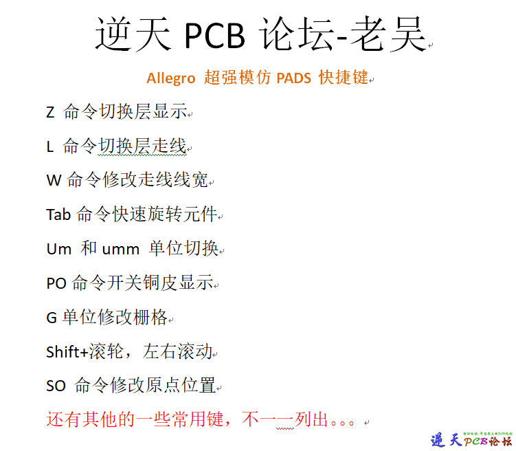 Allegro超强最全模仿PADS快捷键实现Z切换层
 一款NS1068芯片typc-c连接SSD接口的移动硬
 Altera MAX V EP5M570ZF256N开发板PCB文件
 ADI的AD9642评估板PCB文件
 Altera MAX II EPM1270开发板PCB文件
 OWS蓝牙耳机BK方案
 allegro羊皮卷
 从铜丝迷宫到指尖宇宙:揭秘PCBA加工的起源
 LOXIM微孔雾化驱动集成电路原理图_芯片LX82
 这个板子的过孔是怎么做到对这么齐的
 VK0192 LQFP44-LCD驱动原厂-段码屏驱动芯片
 LCD驱动IC段式液晶驱动芯片段码LCD驱动VK16
 导热硅胶片与导热硅脂应该如何选择?


 发表于 2018-11-23 08:54:21


 楼主
楼主
")
")